Total Solution
FULL CHIP DESIGN
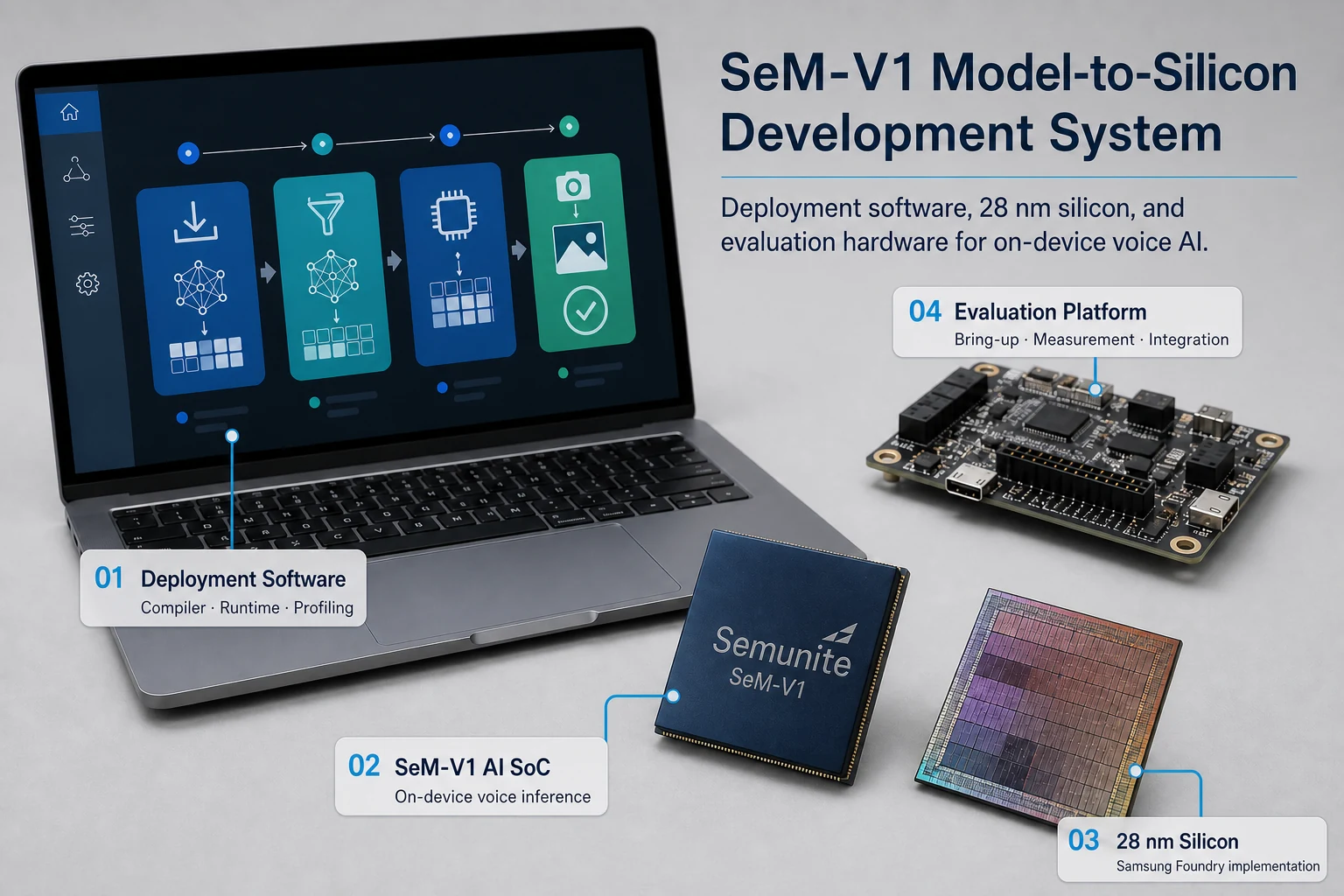
Design / Verification Platform System Architecture Analysis Power Management Control Real Emulation with FPGA IP Supplier Partnership Device Driver, BSP, OS porting
PHYSICAL IMPLEMENTATION
DFT (SCAN / BIST / JTAG) In-system Test STA (Static Timing Analysis) Synthesis & Timing Closure
PHYSICAL DESIGN
Full Chip Floor Plan Hierarchical Physical Design Low Power Design SI Check (IR Drop, Crosstalk-Noise)
PKG & TEST Develop
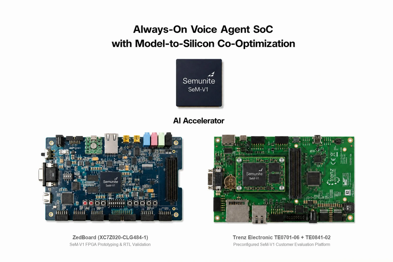
Package Design Test vector generation ATE test set-up Qualification & Reliability Q.A & Failure analysis
Mass Production
Wafer Business Full Turn-key Business (Wafer + PKG + TEST)
PHYSICAL DESIGN
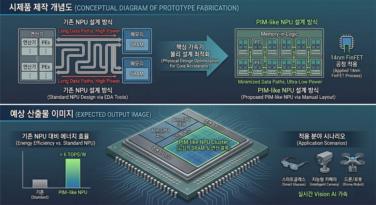
We provide an end-to-end physical-design solution from test through volume production and supply. Long-term strategic partnerships, proven process expertise, and packaging and test experience help customers achieve faster turnaround across the full implementation flow.
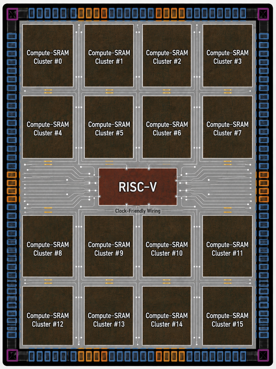
From floorplan
to routed design.
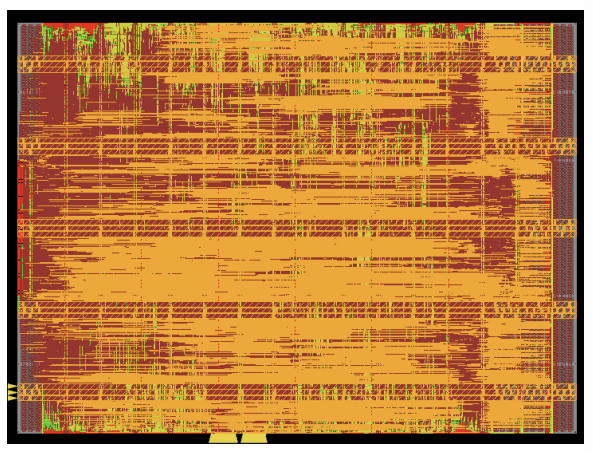
We review hierarchy and routing density from floorplanning through placement and routed implementation. Physical implementation and verification are aligned to the target process and design requirements.
- Placement
- Review physical structure
- Routing
- Inspect routing density
- Review
- Compare implementation results
Advanced Technology